
p-n junction
- noun
- /piː-ɛn ˈdʒʌŋkʃən/
- Specialized
 :
unión p-n
:
unión p-n
- By adjusting the materials used for the p-n junction, engineers can enhance the efficiency of solar panels.
- p-n junction diode
Examples
-
Space-charge layers and an internal electric field form as a result of the diffusion of majority carriers near a p-n junction to the region of opposite conductivity.
Academic text (1993) -
The p-n junction is crucial for the functioning of modern electronic devices like diodes and transistors.
-
The p-n junction diode.
Academic text (1993) -
Although photovoltaic cells come in a variety of forms, the most common structure is a semiconductor material into which a large-area diode, or p-n junction, has been formed.
Academic text (1993) -
Basov was the first scientist in the world to propose the use of semiconductors as the active medium of lasers excited by a variety of methods, including injection across a p-n junction.
Academic text (2002) -
GRAPH: Current-voltage curves for a p-n junction diode in the absence of light and when illuminated. (Adapted from ref. 2; used by permission.)
Academic text (1993) -
The unique electrical properties of the p-n junction allow it to control the flow of current in electronic circuits.
Surface Forms
Morphology
p-n + junction
The noun 'junction' clearly denotes a meeting or boundary, so a learner who recognises 'p' and 'n' as labels could infer this is the meeting of two differently labelled things (partial compositionality). However, 'p-n' is a technical abbreviation referring to semiconductor doping and the important electrical behaviour of the junction is domain-specific and not predictable from the surface constituents, so full understanding requires specialist knowledge.
Etymology
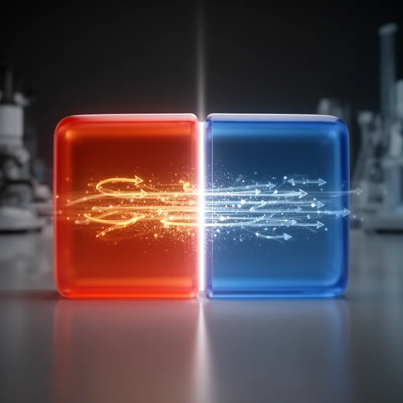
P-n junction is the border where a p-type part (with more 'positive' charge) meets an n-type part (with more 'negative' charge) in a semiconductor. At that border a tiny region acts like a little gate that lets electric current flow easily in 'one direction' but not the other, and that's why devices like diodes and LEDs work.

